10+ vco block diagram
APPLICATIONS JESD204B clock generation. Cellular infrastructure multicarrier GSM LTE W-CDMA Data converter clocking.

Phase Locked Loop Wikiwand
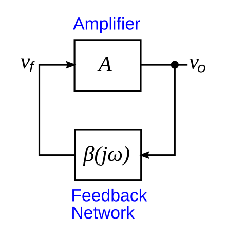
To support this flexibility Skyworks Solutions has created.
. On-board regulators for excellent PSRR. The ADF41513 is packaged in a compact 24-lead 4 mm 4 mm LFCSP. There are several different types.
External VCO input to support up to 6000 MHz. IC-10 IC-Kit for TS-440 R5000 Instuction manualzip. The dielectric films depending on the desired dielectric strength are drawn in a.
The block diagram of a PLL operating as a frequency synthesizer is shown in Figure 1 8. The Institute comprises 33 Full and 13 Associate Members with 12 Affiliate Members from departments within the University of Cape Town and 12 Adjunct Members based nationally or internationally. EUPOL COPPS the EU Coordinating Office for Palestinian Police Support mainly through these two sections assists the Palestinian Authority in building its institutions for a future Palestinian state focused on security and justice sector reforms.
Applications of Voltage Controlled Oscillators VCO Frequency Shift Keying. 68-lead 10 mm 10 mm LFCSP _VQ. For All Hittite PLLs PLL with Integrated VCO Products.
ピアスに関するqa 販売しているピアスはすべて2個売りですか ピアスは2個売りとなっております 一部の特殊な形状のピアスや片耳用のピアスは1個売りとなっております. Receive the latest product releases - click on My. The simplest is an electronic circuit consisting of a variable frequency oscillator and a phase detector in a feedback loopThe oscillators frequency and phase are controlled proportionally by an.
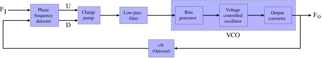
The integrated SYSREF generator outputs single shot N-shot or. Internal VCO Output Frequency Range VCO Gain Control Bit Set High. GENERAL DESCRIPTION The HMC7044.
Phase-Locked Loops VCO GENERAL DESCRIPTION The XR-2206 is a monolithic function generator integrated circuit capable of producing high quality sine square triangle ramp and pulse waveforms of. Manually Generating an Si5351 Register Map for 10-MSOP and 20-QFN Devices 1. The PLL structure consists of a low-power linear VCO and two.
It consists of a reference oscillator OSC a phasefrequency detector PFD a charge pump CP a loop filter LF a voltage-controlled oscillator VCO and two frequency dividers FDs. VOLTAGE CONTROLLED OSCILLATOR VCO FREQUENCY RANGES VCO Output Divide by 1 874 1242 GSPS VCO Output Divide by 2 437 621 GSPS VCO Output Divide by 3 291 414 GSPS PHASE FREQUENCY DETECT INPUT FREQUENCY RANGES 996 GHz VCO Frequency 1087 GHz 25 225 MHz VCO Frequency 996 GHz or 25 770 MHz VCO. Phase array reference distribution.
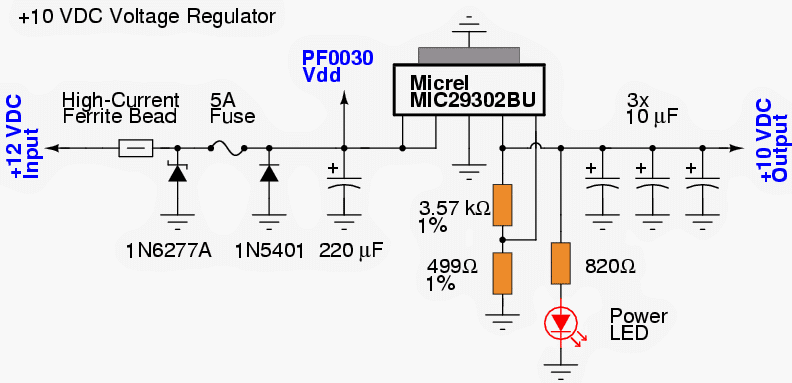
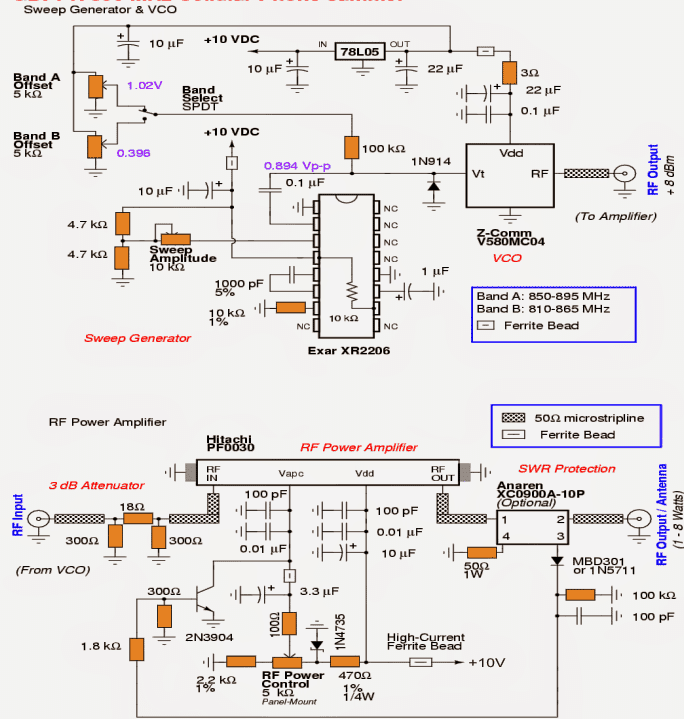
Microwave baseband cards. 20 Alpha Road Chelmsford MA 01824 Phone. XR-2206 Block Diagram 1.
A Versatile Building Block for Micropower Digital and Analog Applications 3 CD4046B PLL Technical Description Figure 2 shows a block diagram of the CD4046B which has been implemented on a single monolithic integrated circuit. The 265 GHz bandwidth eliminates the need for a frequency doubler or divider stage simplifying system architecture and reducing cost. FO e 10 kHz Input Voltage Range Pin 5 4 VCC VCC Average Temperature Coefficient 200 ppmC of Operating Frequency Supply Voltage Rejection 1020V 01 2 V Input Impedance Pin 5 05 1 MX VCO Sensitivity For Pin 5 From 60 66 72 kHzV 810V fO e 10 kHz FM Distortion g10 Deviation 02 15 Maximum Sweep Rate 1 MHz Sweep Range 101.
PLL PLL with Integrated VCO Evaluation Kit. A phase-locked loop or phase lock loop PLL is a control system that generates an output signal whose phase is related to the phase of an input signal. The block diagram and connection diagrams are shown in the figure below.
FUNCTIONAL BLOCK DIAGRAM Figure 1. A cathode-ray tube CRT is a vacuum tube containing one or more electron guns which emit electron beams that are manipulated to display images on a phosphorescent screen. The PLL is a feedback loop that wh en in lock forces.
GENERAL DESCRIPTION The AD9528 is a two-stage PLL with an integrated JESD204B JESD204C SYSREF generator for multiple device synchronization. Film capacitors plastic film capacitors film dielectric capacitors or polymer film capacitors generically called film caps as well as power film capacitors are electrical capacitors with an insulating plastic film as the dielectric sometimes combined with paper as carrier of the electrodes. IDM HS committee meetings for 2022 will be held via Microsoft Teams on the following Tuesdays at 12h30-13h30.
A CRT on a television set is commonly called a picture tube. 4 CD4046B Phase-Locked Loop. Functional block diagram muxout cp out ld sw v com temp ref in clk data le sdv dd avdd dv dd v p ce agnd dgnd cp gnd sd gnd a gndvco r set v vco v tune v ref rf out a rf out a rf out b rf out b phase comparator fast lock switch charge pump output stage output stage pdb rf multiplexer multiplexer 10-bit r counter 2 2 divider doubler.
Technical Brief SWRA029 FractionalInteger-N PLL Basics 5 The problems associated with operating a wireless communications system have become especially acute in the last few years with the advance of cellular telephony and. But in terms of phase its a linear block F Div F VCO N Div Z t 1 F. Software Hardware Installation.
The block diagram consist of a phase detector which acts as a phase comparator an amplifier and a low pass filter with the combination of the resistor 36 kilo ohm and capacitor C2. A block diagram of the Si5351 programmable clock IC is shown in Figure 1. Phase Locked Loop Block Diagram ÖN Ref Div Loop Filter VCO Phase Locked Loops PLL are ubiquitous circuits used in.
The on-chip VCO tunes from 3450 GHz to 4025 GHz. Introduction The Si5351 is a highly flexible and configurable clock generator and VCXO. 001 01 1 10 100-80-40 0 40 Normalized Frequency Magnitude dB 00101 1 10 100-180-135-90-45 0.
This is effected under Palestinian ownership and in accordance with the best European and international standards. Used to build Phase Locked Loops. The ADF5901 24 GHz radar transmitter IC ADF590424 GHz radar 4-channel receiver IC and the ADF4159 FMCW Ramping PLL IC form the basis of the RF chipset which together enable the ADI 24 GHz radar solution.
The images may represent electrical waveforms oscilloscope pictures television set computer monitor radar targets or other phenomena. The value of output frequency is adjustable using the Control voltage on pin 5 with a ratio of 101 which helps us in providing a wide range of control. The output of the amplifier is fed back to the VCO.
104 16 Lead PDIP CDIP 0300 SYMA2 SYMA1 WAVEA2 WAVEA1 GND SYNCO BIAS FSKI AMSI STO MO VCC. An external loop filter and voltage controlled oscillator VCO. FUNCTIONAL BLOCK DIAGRAM 4 500MSPS DDS CORES REF CLOCK INPUT CIRCUITRY TIMING AND CONTROL MODULATION CONTROL SYSTEM CLOCK SOURCE USER INTERFACE RECONSTRUCTED SINE WAVE RECONSTRUCTED.
FUNCTIONAL BLOCK DIAGRAM Figure 1.
How Does Vco In Pll In A Computer Processor Work Quora

Costas Loop Wikiwand

Ne566 Function Generator Voltage Controlled Oscillator Vco Circuit Voltage Controlled Oscillator Function Generator Linear Function

Tracking Range Of Pll And Frequency Range Of Vco Versus Power Supply Download Scientific Diagram

Frequency Synthesizer Wikiwand
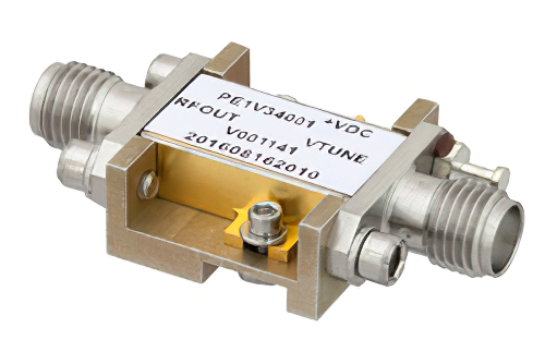
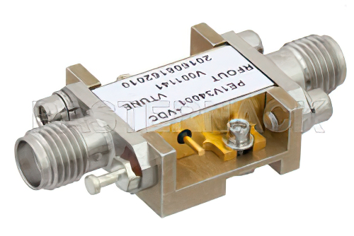
Voltage Controlled Oscillator Vco 5 Ghz To 10 Ghz Phase Noise Of 93 Dbc Hz Hi Rel Hermetic And Sma
Electronic Oscillator Wikiwand

Simple Cd4046 Vco Electronics Projects Diy Circuit Diagram Synthesizer
Phase Locked Loop Wikiwand

Block Diagrams Of A Coherent Ook Receiver With The Injection Locking Download Scientific Diagram

Two Stage Variable Gain Amplifier A Block Diagram B Circuits Of Download Scientific Diagram

Lmc567cn Lmc567cn Original Original Supply Us 0 50 0 50 Audio Ics Ns National Semiconductor Seekic Com
Voltage Controlled Oscillator Vco 5 Ghz To 10 Ghz Phase Noise Of 93 Dbc Hz Hi

Voltage Controlled Oscillator Vco Circuit Voltage Controlled Oscillator Electronic Circuit Projects Circuit
How Does Vco In Pll In A Computer Processor Work Quora
Simple Cellphone Jammer Circuit Homemade Circuit Projects
Simple Cellphone Jammer Circuit Homemade Circuit Projects